Switching the load on and off with one button without locking. Switching the load on and off with one button Switching on with one button
28-07-2016
Anthony Smith
Low-current, momentary switches, similar to board-mounted tact switches, are cheap, readily available, and come in a wide variety of sizes and styles. At the same time, latching buttons are often larger, more expensive, and have a relatively limited range of design options. This can be a problem if you need a miniature, low-cost switch to secure power to a load. The article proposes a circuit solution that allows you to give a self-return button a locking function.
Previously, designs were proposed whose circuits were based on discrete components and microcircuits. However, below we will describe a circuit that requires only a couple of transistors and a handful of passive components to perform the same functions.
Figure 1a shows a variant of the power supply circuit for the case of a load connected to ground. The circuit operates in “switch” mode; this means that the first press turns on the power to the load, the second turns it off, and so on.
To understand the operating principle of the circuit, imagine that the +V S power supply has just been connected, capacitor C1 is initially discharged, and transistor Q1 is turned off. In this case, resistors R1 and R3 are connected in series and pull the gate of P-channel MOSFET Q2 to the +V S bus, keeping the transistor in the closed state. Now the circuit is in an “unblocked” state when the load voltage V L at the OUT (+) pin is zero.
By briefly pressing the normally open button, the gate of Q2 is connected to the capacitor C1, discharged to 0 V, and the MOSFET is turned on. The load voltage at the OUT (+) terminal immediately increases to +VS, through resistor R4, transistor Q1 receives base bias and turns on. As a result, Q1 becomes saturated and connects the gate of Q2 to ground through resistor R3, holding the MOSFET open when the button contacts are open. The circuit is now in a "latched" state where both transistors are open, the load is powered, and capacitor C1 is charged to +V S through resistor R2.
After momentarily closing the switch again, the voltage across capacitor C1 (now equal to +V S) will be applied to the gate of Q2. Since the gate-source voltage of Q2 is now close to zero, the MOSFET turns off and the load voltage drops to zero. Q1's base-emitter voltage also drops to zero, turning off the transistor. As a result, when the button is released, there is nothing holding Q2 open, and the circuit returns to the "enabled" state, with both transistors turned off, the load de-energized, and C1 discharged through resistor R2.
It is not necessary to install the resistor R5 that shunts the output terminals. When the button is released, capacitor C1 is discharged to the load through resistor R2. If the load impedance is very high (that is, comparable to the value of R2), or the load contains active devices such as, say, LEDs, the load voltage when Q2 is turned off may be large enough to turn on transistor Q1 through resistor R4 and prevent the circuit from switch off. Resistor R5, when Q2 turns off, pulls the OUT (+) terminal to the 0V rail, causing Q1 to turn off quickly and allowing the circuit to properly transition to the off state.
With the right selection of transistors, the circuit will operate over a wide range of voltages and can be used to drive loads such as relays, solenoids, LEDs, etc. However, keep in mind that some DC fans and motors continue to spin after the power is turned off. This rotation can create a back emf large enough to turn on transistor Q1 and prevent the circuit from turning off. The solution to the problem is shown in Figure 1b, where a blocking diode is connected in series with the output. In this case, you can also add resistor R5 to the circuit.
Figure 2 shows another circuit designed for loads connected to the top power rail, such as the electromagnetic relay shown in this example.
Note that Q1 has been replaced by a pnp transistor, and Q2 is now an N-channel MOSFET. This circuit works exactly the same as the circuit described above. Here, R5 acts as a pull-up resistor, connecting the OUT (-) output pin to the +V S bus when Q2 turns off, and causing Q1 to turn off quickly. As in the previous circuit, resistor R5 is an optional component, and is installed only for certain types of loads mentioned above.
Note that in both circuits the time constant C1, R2 is selected based on the required contact bounce suppression. Typically, a value from 0.25 s to 0.5 s is considered normal. Smaller time constants can lead to unstable operation of the circuit, while larger ones increase the waiting time between closing the button contacts, during which a sufficiently complete charge and discharge of capacitor C1 must occur. With the values indicated in the diagram C1 = 330 nF and R2 = 1 MOhm, the nominal value of the time constant is 0.33 s. Usually this is enough to eliminate contact bounce and switch the load in about a couple of seconds.
Both circuits are designed to latch and release the key in response to momentary contact closures. However, each of them was designed in such a way as to guarantee correct operation even when the button is pressed for any length of time. Consider the circuit in Figure 2 when Q2 is off. If the button is pressed to turn off the circuit, the gate is connected to the 0V potential (since capacitor C1 is discharged) and the MOSFET is closed, allowing the common point of resistors R1 and R2 to connect to the +V S rail through resistor R5 and the load impedance. At the same time, Q1 is also turned off, causing the gate of Q2 to be connected to the GND bus through resistors R3 and R4. If the button is immediately released, C1 will simply charge through resistor R2 to a voltage of +V S. However, if you leave the button closed, the gate voltage of Q2 will be determined by the potential of the divider formed by resistors R2 and R3+R4. Assuming that when the circuit is unlocked, the voltage at the OUT (-) pin is approximately equal to +V S, the following expression can be written for the gate-source voltage of transistor Q2:
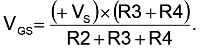
Even if the +V S voltage is 30 V, the resulting 0.6 V voltage between gate and source is not enough to turn the MOSFET back on. Therefore, when the button contacts are open, both transistors will remain off.
Radio amateur Power supplyOne button switch on and off
Turn on and off with just one button
In radio electronics, situations arise when one or several loads require only one button that will turn the power on and off. This approach has advantages over placing two buttons or volumetric toggle switches in the case. It is also possible to use stylish and compact touch buttons. Or use one-button switching on and off in cases where there is only one button. Two schemes will be considered, in different designs and with different power options. Both options are working and tested. If the components were installed correctly and without replacing parts, then everything will work properly.
On and off one button - circuit on the trigger

The power supply for the circuit ranges from 7 V to 35 V. All parts are inexpensive, and repetition of the circuit can be done by people far from radio electronics. You can use any button, even for calls, as long as it can connect and disconnect a contact. You can hold it as long as you like, since the trigger will only work when the contact is disconnected. Accordingly, it will enter the next position when pressed again.


On and off one button - circuit on timer 555
Another remarkable circuit is based on the 555 timer. It is notable for the fact that the supply voltage is mains, and several loads can be connected, as well as buttons. The diagram shows the locations of subsequent connections.

Many household electrical appliances, be it stereo systems, televisions, various lamps, are turned on and off by pressing the same button. Pressed once - the device turned on, pressed again - turned off. In amateur radio practice there is often a need to implement the same principle. Such buttons are often used when building homemade amplifiers in elegant cases; a device with this principle of switching on and off looks much more advanced, reminiscent of a factory device.
Device diagram
The diagram for turning the load on and off with one button is presented below. It is as simple as boots, does not contain scarce components and starts up immediately. So, the diagram:
Its key link is the popular NE555 timer chip. It is this that registers the key press and sets the output to either logical 1 or 0. Button S1 is any button for closing without fixing, because There is practically no current flowing through it, there are practically no requirements for the button. I took the first one I came across, a Soviet one from the 60s.

Capacitor C1 and resistor R3 suppress the bounce of the button contacts; C1 is best used non-polar ceramic or film. LED1 indicates the state of the load - the LED is on, the load is on, off - off. Transistor T1 switches the relay winding; here you can use any low-power transistor of the NPN structure, for example, BC547, KT3102, KT315, BC184, 2N4123. A diode placed parallel to the relay winding serves to suppress self-induction pulses arising in the winding. You can use any low-power diode, for example, KD521, 1N4148. If the load consumes little current, you can connect it directly to the circuit instead of the relay coil. In this case, it is worth installing a more powerful transistor, for example, KT817, and the diode can be eliminated.
Materials

To assemble the circuit you will need:
- Chip NE555 – 1 pc.
- Transistor BC547 – 1 pc.
- Capacitor 1 uF - 1 pc.
- Resistor 10 kOhm – 2 pcs.
- Resistor 100 kOhm – 1 pc.
- Resistor 1 kOhm – 2 pcs.
- Button without fixation – 1 pc.
- Diode KD521 – 1 pc.
- LED 3 V. - 1 PC.
- Relay – 1 pc.
Assembling the device
First of all, you need to make a printed circuit board. It is performed using the LUT method, the file is attached to the article. There is no need to mirror before printing. The LUT method has been described several times on the Internet; learning it is not so difficult. A few photos of the process:Download the board:
(downloads: 958)


If you don’t have a printer at hand, you can draw a printed circuit board with a marker or varnish, because it is quite small. After drilling the holes, the board must be tinned to prevent oxidation of the copper traces.
After making the board, you can start soldering parts into it. First, small components are soldered - resistors, diodes. After that, capacitors, microcircuits and everything else. The wires can be either soldered directly into the board or connected to the board using terminal blocks. I brought out the power contacts and OUT contacts for connecting the relay through terminal blocks, and soldered the button directly into the board using a pair of wires.

Thus, this board can be built into any device, be it an amplifier, a homemade lamp, or anything else that requires turning it on and off with one button without locking. There are many other similar circuits on the network, built on Soviet microcircuits and transistors, but this particular circuit using the NE555 microcircuit has proven itself to be the simplest and at the same time reliable.

Sometimes there is a need to control a particular load with just one button. There are two types of buttons, with and without latching. If you use non-latching buttons, for example to turn on an LED, then when pressed the LED will light up and when released it will go out.
The above circuit is incredibly simple and consists of three transistors, two of which are of reverse conductivity. It works according to the following principle: when pressed for the first time, the LED will light up, and when pressed again, it will go out.
There are many areas of application for such a simple electronic button, from simple flashlights to powerful switching systems.
How it works
At the initial moment, when power is supplied to the circuit, all three transistors are closed, at the same time, through the chain of resistors R1 and R2, the electrolytic capacitor C1 is charged, the voltage on it is equal to the supply voltage. When you press the button, a positive signal from the capacitor is sent to the base of transistor VT3, unlocking it; through the open transition of this transistor, voltage is supplied to the base of transistor VT2, as a result of which it also opens. The load, in our case the LED, is also activated, even during the operation of the transistor VT3.
This part of the circuit is a trigger latch. Transistor VT3 opens VT2, and when it opens, it supplies voltage to the base of transistor VT3, keeping it open.
The circuit can remain in this state for an infinitely long time. Moreover, the button can simply be pressed and released, rather than held down.
The opening transistor VT2 also opens the transistor VT1. In this state, all three transistors are open. When VT1 is open, through its open junction and resistor R2, capacitor C1 will be discharged, hence we can conclude that when the transistors are open, the capacitor is discharged.
When the button is pressed again, the base of the transistor VT3 is connected to the negative plate of the capacitor C1, at the base of the key the voltage is around 0.7 volts, and as a result of the charge of the capacitor it drops and it is locked. With transistor VT3 turned off, the capacitor again begins to charge in normal mode, through the previously specified resistors.
The load is switched by transistor VT3, it can be taken more powerfully, for example bd139, in this case we will have the opportunity to connect more powerful loads to the circuit, or we can amplify the signal from the output of our button with an additional transistor.
The transistors used in the circuit are not critical; you can take any low and medium power of appropriate conductivity. The values of other components of the circuit can be deviated in one direction or another by 30%.
The circuit is not power-hungry; from a 5-volt power source, the no-load current consumption is only 850 microAmps, so that you can safely use it as a switch in, say, a flashlight.